
[ad_1]
From the angle of a standard x86 computing fanatic—or skilled—mainframes are unusual, archaic beasts. They’re bodily monumental, power-hungry, and costly by comparability to extra conventional data-center gear, typically providing much less compute per rack at the next value.
This raises the query, “Why preserve utilizing mainframes, then?” When you hand-wave the cynical solutions that boil all the way down to “as a result of that is how we have all the time executed it,” the sensible solutions largely come all the way down to reliability and consistency. As AnandTech’s Ian Cutress factors out in a speculative piece targeted on the Telum’s redesigned cache, “downtime of those [IBM Z] methods is measured in milliseconds per yr.” (If true, that is at the least seven nines.)
IBM’s personal announcement of the Telum hints at simply how completely different mainframe and commodity computing’s priorities are. It casually describes Telum’s reminiscence interface as “able to tolerating full channel or DIMM failures, and designed to transparently get well information with out affect to response time.”
Whenever you pull a DIMM from a dwell, working x86 server, that server doesn’t “transparently get well information”—it merely crashes.
IBM Z-series structure
Telum is designed to be one thing of a one-chip-to-rule-them-all for mainframes, changing a way more heterogeneous setup in earlier IBM mainframes.
The 14 nm IBM z15 CPU that Telum is changing options 5 complete processors—two pairs of 12-core Compute Processors and one System Controller. Every Compute Processor hosts 256MiB of L3 cache shared between its 12 cores, whereas the System Controller hosts a whopping 960MiB of L4 cache shared between the 4 Compute Processors.
5 of those z15 processors—every consisting of 4 Compute Processors and one System Controller—constitutes a “drawer.” 4 drawers come collectively in a single z15-powered mainframe.
Though the idea of a number of processors to a drawer and a number of drawers to a system stays, the structure inside Telum itself is radically completely different—and significantly simplified.
Telum structure
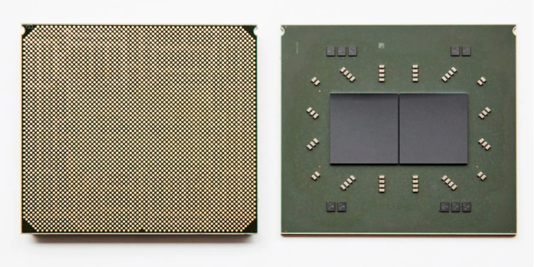
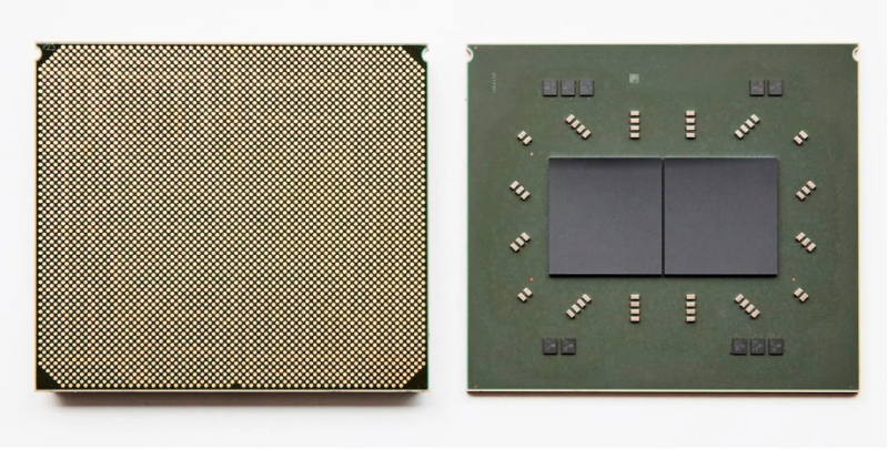
Telum is considerably less complicated at first look than z15 was—it is an eight-core processor constructed on Samsung’s 7nm course of, with two processors mixed on every bundle (much like AMD’s chiplet method for Ryzen). There isn’t a separate System Controller processor—all of Telum’s processors are similar.
From right here, 4 Telum CPU packages mix to make one four-socket “drawer,” and 4 of these drawers go right into a single mainframe system. This supplies 256 complete cores on 32 CPUs. Every core runs at a base clockrate over 5 GHz—offering extra predictable and constant latency for real-time transactions than a decrease base with greater turbo fee would.
Pockets stuffed with cache
Taking away the central System Processor on every bundle meant redesigning Telum’s cache, as properly—the large 960MiB L4 cache is gone, in addition to the per-die shared L3 cache. In Telum, every particular person core has a non-public 32MiB L2 cache—and that is it. There isn’t a {hardware} L3 or L4 cache in any respect.
That is the place issues get deeply bizarre—whereas every Telum core’s 32MiB L2 cache is technically non-public, it is actually solely nearly non-public. When a line from one core’s L2 cache is evicted, the processor seems to be for empty area within the different cores’ L2. If it finds some, the evicted L2 cache line from core x is tagged as an L3 cache line and saved in core y‘s L2.
OK, so we now have a digital, shared up-to-256MiB L3 cache on every Telum processor, composed of the 32MiB “non-public” L2 cache on every of its eight cores. From right here, issues go one step additional—that 256MiB of shared “digital L3” on every processor can, in flip, be used as shared “digital L4” amongst all processors in a system.
Telum’s “digital L4” works largely the identical means its “digital L3” did within the first place—evicted L3 cache traces from one processor search for a house on a unique processor. If one other processor in the identical Telum system has spare room, the evicted L3 cache line will get retagged as L4 and lives within the digital L3 on the opposite processor (which is made up of the “non-public” L2s of its eight cores) as an alternative.
AnandTech’s Ian Cutress goes into extra element on Telum’s cache mechanisms. He ultimately sums them up by answering “How is that this potential?” with a easy “magic.”
AI inference acceleration
https://www.youtube.com/watch?v=TRBgBbvYiQw
IBM’s Christian Jacobi briefly outlines Telum’s AI acceleration on this two-minute clip.
Telum additionally introduces a 6TFLOPS on-die inference accelerator. It is meant for use for—amongst different issues—real-time fraud detection throughout monetary transactions (versus shortly after the transaction).
Within the quest for max efficiency and minimal latency, IBM threads a number of needles. The brand new inference accelerator is positioned on-die, which permits for decrease latency interconnects between the accelerator and CPU cores—but it surely’s not constructed into the cores themselves, a la Intel’s AVX-512 instruction set.
The issue with in-core inference acceleration like Intel’s is that it usually limits the AI processing energy obtainable to any single core. A Xeon core working an AVX-512 instruction solely has the {hardware} inside its personal core obtainable to it, which means bigger inference jobs have to be cut up amongst a number of Xeon cores to extract the complete efficiency obtainable.
Telum’s accelerator is on-die however off-core. This enables a single core to run inference workloads with the would possibly of the total on-die accelerator, not simply the portion constructed into itself.
Itemizing picture by IBM
[ad_2]
Source link


